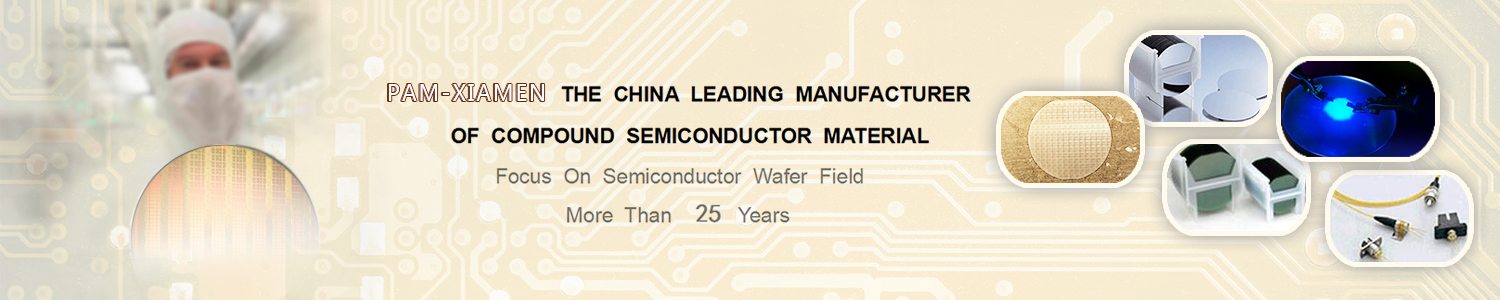
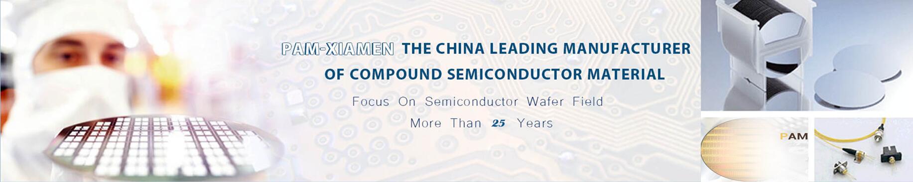
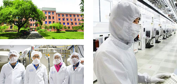
Les gabarits de pam-xiamen sont constitués de couches cristallines de nitrure de gallium (gan), de nitrure d'aluminium (aln), de nitrure d'aluminium gallium (algan) et de nitrure d'indium et de gallium (ingan) déposées sur des substrats de saphir, Les produits modèles en carbure de silicium ou silicium.pam-xiamen permettent des durées de cycle d'ép3
pam-xiamen a établi la technologie de fabrication de la plaquette de substrat gan (nitrure de gallium) autoportante, qui est pour uhb-led et ld. développé par la technologie d'épitaxie en phase vapeur (hvpe), notre substrat gan a une faible densité de défauts.
pwam développe et fabrique des substrats semi-conducteurs composés de cristaux d'arséniure de gallium et wafer.we a utilisé une technologie avancée de croissance cristalline, congélation verticale gradient (vgf) et gaas gaufrage technologie de traitement, établi une ligne de production de croissance de cristal, de coupe, de broyage à polissage une 3
nous fournissons une épitaxie sic sur film mince (carbure de silicium) sur des substrats de 6h ou 4h pour le développement de dispositifs en carbure de silicium. sic epi wafer est principalement utilisé pour les diodes schottky, les transistors à effet de champ à semi-conducteur à oxyde de métal, les transistors à effet de champ de jonction, les tr3
pam-xiamen propose des plaquettes de carbure de silicium semi-conducteur, 6h sic et 4h sic dans différentes qualités pour le chercheur et les fabricants de l'industrie. nous avons développé la technologie de croissance de cristal de sic et la technologie de traitement de gaufrette de cristal de sic, établi une ligne de production au substrat sic fa3
La plaquette épitaxiale à base de gan (nitrure de gallium) de pam-xiamen est destinée à l'application de diodes électroluminescentes bleues et vertes à très haute luminosité (led) et de diodes laser (ld).
Les nitrures de gallium (gan) (transistors à haute mobilité d'électrons) sont la prochaine génération de transistors de puissance. Grâce à la technologie gan, pam-xiamen offre maintenant une plaquette algan / gan hemt epi sur saphir ou silicone, et algan / gan sur saphir .
pam-xiamen est en mesure d'offrir les services suivants de plaquettes de récupération de sic.
vous pouvez obtenir notre service de technologie libre de l'enquête à après service basé sur notre 25+ expériences dans la ligne de semi-conducteur.
notre objectif est de répondre à toutes vos exigences, peu importe comment les petites commandes et comment les questions difficiles ils peuvent être, pour maintenir une croissance soutenue et rentable pour chaque client grâce à nos produits qualifiés et un service satisfaisant.
avec plus de 25 + ans expériences Dans le domaine des matériaux semi-conducteurs composés et l'exportation, notre équipe peut vous assurer que nous pouvons comprendre vos besoins et traiter votre projet de manière professionnelle.
la qualité est notre première priorité. pam-xiamen a été iso9001: 2008 , possède et partage quatre facettes modernes qui peuvent fournir une gamme assez large de produits qualifiés pour répondre aux différents besoins de nos clients, et chaque commande doit être traitée par notre système de qualité 3
Poly-Si crystals are mainly used in solar cells because of their low cost. Here, the zones of sensitivity to wavelengths in sunlight should be expanded to increase the engineering efficiency of solar cells. Group IV compound semiconductors films, e.g., Si (Ge) films doped with C, Ge (C, Si), and/or Sn atoms with contents of several %, on a Si or Ge substrate have been identified as potential solutions to this technical problem. In this study, we calculated the formation energy of each atomic configuration of C, Ge, and Sn atoms in Si by using density functional theory. The "Hakoniwa" method proposed by Kamiyama et al. [Materials Science in Semiconductor Processing, 43, 209 (2016)] was applied to a 64-atom supercell of Si including up to three atoms of C, Ge, and/or Sn (up to 4.56%) in order to obtain the ratio of each atomic configuration and the average value of the Si bandgaps. Not only the conventional generalized gradient approximation (GGA) but also the screened-exchange local-den...
Lire la suiteSource:IOPscience For more information, please visit our website: www.semiconductorwafers.net, send us email at sales@powerwaywafer.com or powerwaymaterial@gmail.com
Lire la suiteThe optical transmission, temperature-dependence of the photoluminescence (PL), and Raman scattering of porous SiC prepared from p-type 6H-SiC are compared with those from bulk p-type 6H-SiC. While the transmission spectrum of bulk SiC at room temperature reveals a relatively sharp edge corresponding to its band gap at 3.03 eV, the transmission edge of porous SiC (PSC) is too wide to determine its band gap. It is believed that this wide edge might be due to surface states in PSC. At room temperature, the PL from PSC is 20 times stronger than that from bulk SiC. The PL PSC spectrum is essentially independent of temperature. The relative intensities of the Raman scattering peaks from PSC are largely independent of the polarization configuration, in contrast to those from bulk SiC, which suggests that the local order is fairly random. Source:IOPscience For more information, please visit our website: www.semiconductorwafers.net, send us email at sales@powerwaywafer.com&...
Lire la suite1−y alloy as the annealing source.
Lire la suiteIn this study, an InP layer was transferred onto a Si substrate coated with a thermal oxide, through a process combining ion-cutting process and selective chemical etching. Compared with conventional ion-cutting of bulk InP wafers, this layer transfer scheme not only takes advantage of ion- cutting by saving the remaining substrates for reuse, but also takes advantage of selective etching to improve the transferred surface conditions without using the chemical and mechanical polishing. An InP/InGaAs/InP heterostructure initially grown by MOCVD was implanted with H+ ions. The implanted heterostructure was bonded to a Si wafer coated with a thermal SiO2 layer. Upon subsequent annealing, the bonded structure exfoliated at the depth around the hydrogen projected range located in the InP substrate. Atomic force microscopy showed that after selective chemical etchings on the as-transferred structure, a final structure of InP/SiO2/Si was obtained with a relatively smooth surface. Source:IOPsc...
Lire la suiteWe review our recent efforts on developing HgCdSe infrared materials on GaSb substrates via molecular beam epitaxy (MBE) for fabricating next generation infrared detectors with features of lower production cost and larger focal plane array format size. In order to achieve high-quality HgCdSe epilayers, ZnTe buffer layers are grown before growing HgCdSe, and the study of misfit strain in ZnTe buffer layers shows that the thickness of ZnTe buffer layer needs to be below 300 nm in order to minimize the generation of misfit dislocations. The cut-off wavelength/alloy composition of HgCdSe materials can be varied in a wide range by varying the ratio of Se/Cd beam equivalent pressure during the HgCdSe growth. Growth temperature presents significant impact on the material quality of HgCdSe, and lower growth temperature leads to higher material quality for HgCdSe. Typically, long-wave infrared HgCdSe (x=0.18, cut-off wavelength of at 80 K) presents an electron mobility as high as&nbs...
Lire la suiteWet etching is an important step in the manufacturing of semiconductor and solar wafers and for the production of MEMS devices. While it has been replaced by the more precise dry etching technology in advanced semiconductor device fabrication, it still plays an important role in the manufacture of the silicon substrate itself. It is also used for providing stress relief and surface texturing of solar wafers in high volume. The technology of wet etching silicon for semiconductor and solar applications will be reviewed. Impact on this step for wafer properties and critical parameters (flatness, topology and surface roughness for semiconductor wafers, surface texture and reflectance for solar wafers) will be presented. The rationale for the use of a etching technology and etchant for specific applications in semiconductor and solar wafer manufacturing will be presented. Source:IOPscience For more information, please visit our website: www.semiconductorwafers.net, send us email at&nbs...
Lire la suite4H-SiC homoepitaxial films were grown on 8° off-axis porous 4H-SiC (0001) faces in the temperature range of by chemical vapor deposition from bis(trimethylsilyl)methane (BTMSM) precursor. The activation energy for growth was 5.6 kcal/mol, indicating that the film growth is dominated by the diffusion-limited mechanism. Triangular stacking faults were incorporated in the SiC thin film grown at low temperature of 1280°C due to the formation of 3C-SiC polytype. Moreover, super-screw dislocations appeared seriously in the SiC film grown below 1320°C. Clean and featureless morphology was observed in the SiC film grown below 25 standard cubic centimeters per minute (sccm) carrier gas flow rate of BTMSM at 1380°C while 3C-SiC polytype with double positioning boundaries grew at 30 sccm flow rate of BTMSM. The dislocation density of the epi layer was strongly influenced by the growth temperature and flow rate of BTMSM. Double axis crystal X-ray diffraction and optical micro...
Lire la suiteDuring the last decade, the use of single crystal germanium (Ge) layers and structures in combination with silicon (Si) substrates has led to a revival of defect research on Ge. In Si crystals, dopants and stresses affect the intrinsic point defect (vacancy V and self-interstitial I) parameters and thus change the thermal equilibrium concentrations of V and I Source:IOPscience For more information, please visit our website: www.semiconductorwafers.net, send us email at sales@powerwaywafer.com or powerwaymaterial@gmail.com
Lire la suiteOffice Address: #506B, Henghui Business Center, No.77, Lingxia Nan Road, High Technology Zone, Huli, Xiamen, 361006